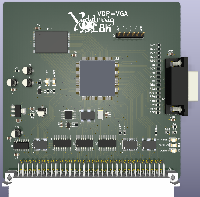
VGA card redesigned
Another change that hasnt been documented until now is an incremental but meaningful update to my FPGA-based graphics card. The original board was designed several years ago using Proteus, and while it has worked well, it was the only board that hadn’t been moved over to KiCAD.
The main motivation for this update was to migrate the design from Proteus to KiCad. Converting the schematic wasn’t too difficult, but as I was rebuilding the board anyway, it became a good opportunity to make some small improvements to the design. Some of these changes came about from a better understanding of the FPGA and what pins could be reused after startup such and the mode and SPI pins.
The original board was using 12-bit colour, the VGA output path has been expanded from the 12-bit (4:4:4 RGB) to 16-bit (5:6:5 RGB) colour that allows 65,536 colours instead of 4,096. Having more free pins available has also allowed me to expand the address range directly accessible from the CPU.
The previous board only allowed the 68k to map 256KB of the video SRAM at once, relying on banking for access to the full memory. The new revision extends that to a 1MB CPU-accessible window, reducing the amount of bank switching needed and making VRAM updates far more straightforward.
While the hardware changes were fairly minor, there has been a lot of changes to the VHDL code for the FPGA. In the previous version, the bitmap modes were working well but the code was becoming a mess and the design was not easily expandable. The decision was made to go back to basics and redesign the code to make it mode modular and expandable.
This change took the card back having two video modes:
- 80x30 character text mode with a fixed palette of 16 colours and 16 background colours per character.
- 640x480 16-bpp framebuffer bitmap mode
One of the big changes that I wanted to make when redesigning the code was to improve the memory access for the bitmap mode. The previous version was fetching the data for each pixel as it was required so this meant that the SRAM controller had to be able fetch the data on exact timing intervals. This made the SRAM access a little fragile and easy to break. The solution to this was to use a FIFO buffer to start fetching the data for the next visible line during the display blanking periods. With this change, it ensures that display has a constant supply of pixels and that the SRAM can be updated without having to worry about breaking display timing requirements.
This gave me a good and reliable starting point for expanding the design.
