PCB Problems
I’ve started assembling the first board, but immediately ran into a serious issue: there was a short between the 5 V and GND planes on the bare PCBs.
Tracking it down took some time (and the sacrifice of a couple of boards), but by cutting them apart I was able to narrow the fault’s location.
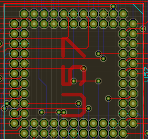
The root cause turned out to be several vias that had no clearance from the internal power planes. Strangely, this didn’t show up when checking the files in a Gerber viewer — everything looked correct, with proper clearance around the vias.

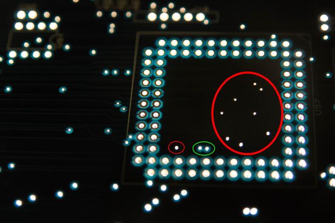
To confirm, I backlit the board with a strong light. This made the problem areas obvious: the vias highlighted in green were fine, but the ones marked red were shorting directly into the inner layers. Drilling out these vias removed the short.

Ultimately, the issue was traced back to the manufacturer’s CAM software misinterpreting the Gerber files. Since a working set couldn’t be generated, they refunded the cost of the boards.