Address Decoding
Before any software can run on Y Ddraig, the CPLD needs to be programmed. I’m using a Xilinx XC95108, which handles address decoding for the system peripherals. Later on, it will also take over DRAM control, but for now I’m keeping things simple and focusing on getting the machine up and running without DRAM.
Clock generator #
The CPLD also generates the 68000’s clock signal. The first step is to create a stable clock for the CPU: a 10 MHz output clock derived from the 40 MHz input fed into the CPLD.
architecture Behavioral of Clock is
	signal clk_divider : std_logic_vector(1 downto 0) := (others => '0');
begin
	process(clk)
	begin
		if (rising_edge(clk)) then
			clk_divider <= clk_divider + 1;
		end if;
	end process;

	clk10 <= clk_divider(1);
end Behavioral;
Address decoding #
The memory map for Y Ddraig is laid out as follows:
| Device | Start Address | End Address |
|---|---|---|
| Static Ram | 0x000000 | 0x0FFFFF |
| Dynamic RAM | 0x100000 | 0x900000 |
| DUART | 0xF7F000 | 0xF7F0FF |
| YM2151 | 0xF7F100 | 0xF7F1FF |
| PIT | 0xF7F200 | 0xF7F2FF |
| KBD | 0xF7F300 | 0xF7F3FF |
| IDE | 0xF7F400 | 0xF7F4FF |
| ETHERNET | 0xF7F500 | 0xF7F5FF |
| RTC | 0xF7F600 | 0xF7F6FF |
| VDP | 0xF7F700 | 0xF7F7FF |
| ROM | 0xF80000 | 0xFFFFFF |
On reset, the 68000 expects to fetch its initial stack pointer and program counter from address 0x000000. Since the ROM is actually mapped at 0xF80000, those first four reads need to be redirected to the ROM.
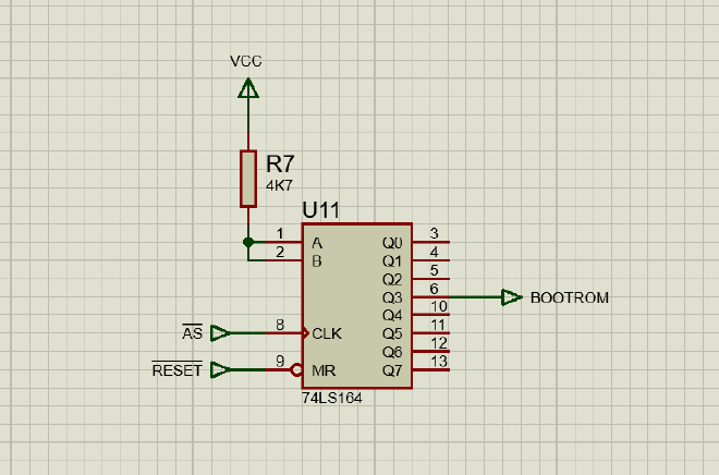
This is handled by a 74LS164 8-bit shift register (U11), which pulls the bootrom signal low for the first four address strobes (/AS). After that, the signal stays high until the next reset, allowing normal RAM operation.

With this in place, the address decoder can be defined in VHDL.
entity AddressDecode is
    Port ( a          : in  STD_LOGIC_VECTOR (23 downto 8);
           clk        : in  STD_LOGIC;
           as         : in  STD_LOGIC;
           bootrom    : in  STD_LOGIC;
           reset      : in  STD_LOGIC;
           dtack      : out  STD_LOGIC;
           cs_rom     : out  STD_LOGIC;
           cs_sram    : out  STD_LOGIC;
           cs_duart   : out  STD_LOGIC;
           cs_pit     : out  STD_LOGIC;
           cs_kbd     : out  STD_LOGIC;
           cs_rtc     : out  STD_LOGIC;
           cs_ym2151  : out  STD_LOGIC;
           cs_eth     : out  STD_LOGIC;
           cs_vdp     : out  STD_LOGIC;
           cs_ide     : out  STD_LOGIC);
end AddressDecode;
ROM is selected whenever the bootrom signal is low, or if the address falls within the ROM range. Similarly, RAM is only enabled when bootrom is high, ensuring the startup vectors are always fetched from ROM.
Peripheral devices are mapped in 256-byte windows within the ranges shown above.
-- $F80000 - $FFFFFF
cs_rom    <= '0' WHEN as = '0'
    AND (bootrom = '0' OR std_match(a, "11111-----------"))
    ELSE '1';

-- $000000 - $0FFFFF
cs_sram   <= '0' WHEN as = '0'
    AND bootrom = '1' AND std_match(a, "0000------------")
    ELSE '1';

-- $F7F000 - $F7F0FF
cs_duart    <= '0' WHEN as = '0' AND std_match(a, "1111011111110000") ELSE '1';
-- $F7F100 - $F7F1FF
cs_ym2151   <= '0' WHEN as = '0' AND std_match(a, "1111011111110001") ELSE '1';
-- $F7F200 - $F7F2FF
cs_pit      <= '0' WHEN as = '0' AND std_match(a, "1111011111110010") ELSE '1';
-- $F7F300 - $F7F3FF
cs_kbd      <= '0' WHEN as = '0' AND std_match(a, "1111011111110011") ELSE '1';
-- $F7F400 - $F7F4FF
cs_ide      <= '0' WHEN as = '0' AND std_match(a, "1111011111110100") ELSE '1';
-- $F7F500 - $F7F5FF
cs_eth      <= '0' WHEN as = '0' AND std_match(a, "1111011111110101") ELSE '1';
-- $F7F600 - $F7F6FF
cs_rtc      <= '0' WHEN as = '0' AND std_match(a, "1111011111110110") ELSE '1';
-- $F7F700 - $F7F7FF
cs_vdp      <= '0' WHEN as = '0' AND std_match(a, "1111011111111111") ELSE '1';
For some devices, DTACK is automatically provided (the DUART and the PIT). For others, DTACK needs to be generated in logic.
The DTACK generator:
signal dtack_s  : std_logic_vector(3 downto 0);

process (clk, reset, as)
begin
	if (reset = '0' or as = '1') then
		dtack_s <= (others => '0');
	elsif (rising_edge(clk)) then
		if (dtack_s < "1111") then
			dtack_s <= dtack_s + 1;
		end if;
	end if;
end process;
Check if we need to generate the DTACK signal:
-- Check the chip select signals to see if one is low
ack <= cs_sram AND cs_kbd AND cs_rtc AND cs_ym2151 AND cs_vdp AND cs_eth;

-- Generate the DTACK
dtack <= '0' WHEN ack = '0' AND dtack_s > "0101" ELSE '1';
With this address decode logic in place, the hardware should now be accessible, and I can begin writing code to test and verify each device.