PCB design re-started
After a long break from the project I have decided to restart the design making a few changes to the board.
When trying to get the inital board working if found a manufacturing error on the PCB which required drilling out some VIAs and adding some link wires creating a very messy start to the project.
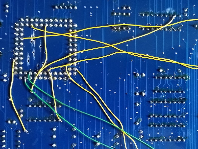
Along with trying to fix this problem I discovered a couple of design related issues that I had made. Due to these and fact that I didn’t have the required time to spend working on this I lost the motivation to do any work on the board.
After returning to the project I had some different ideas that I wanted to incorporate on the board so it seemed to be a good opportunity to work on a redesign as the original wasn’t even close to working at this point anyway.
Currently working on the new schematic which will be posted once I’m happy with the design.