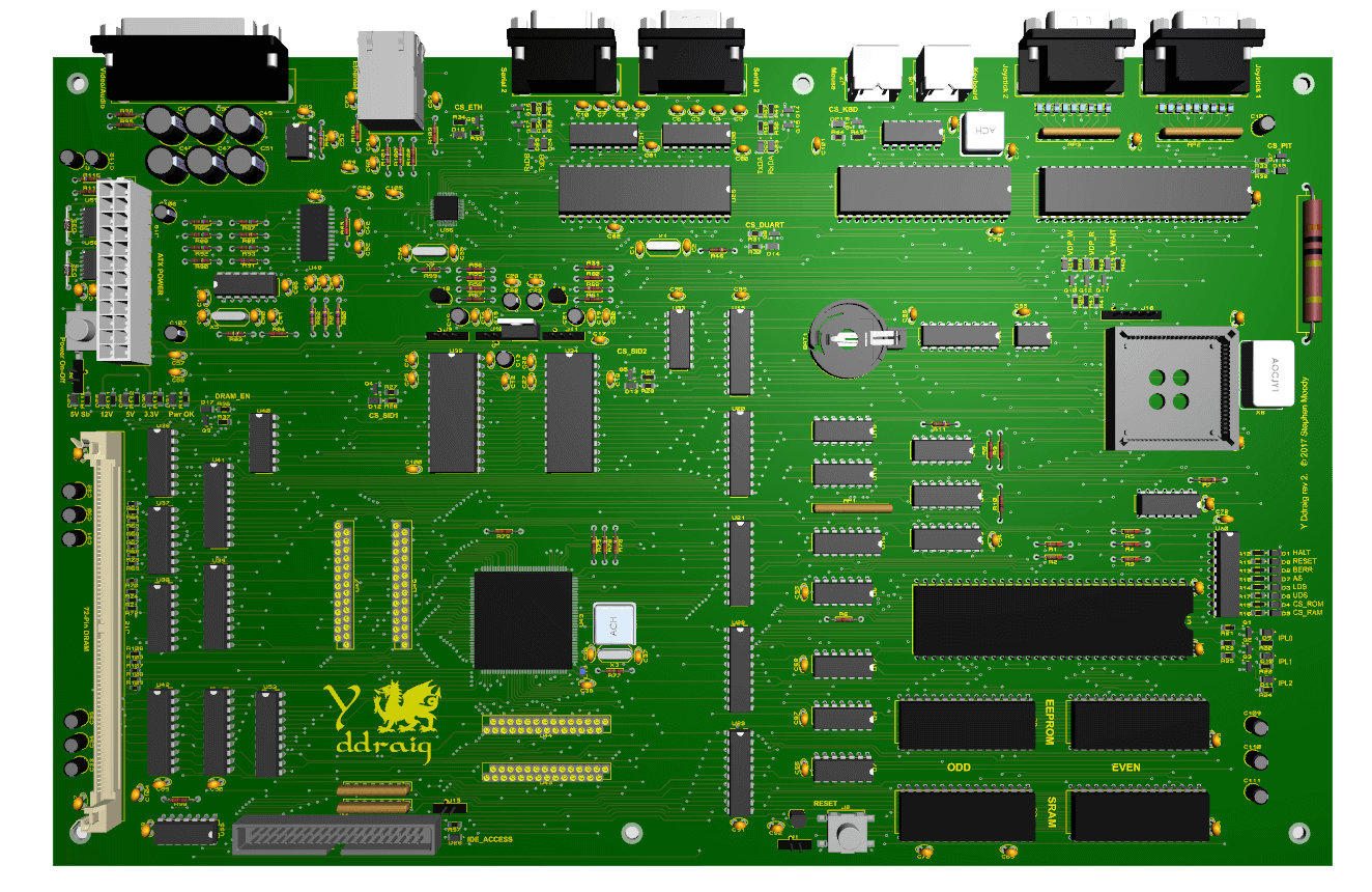
PCB design completed
The schematic design has been done and after many hours routing tracks the PCB layout has been completed and ready to be sent off for manufacture.
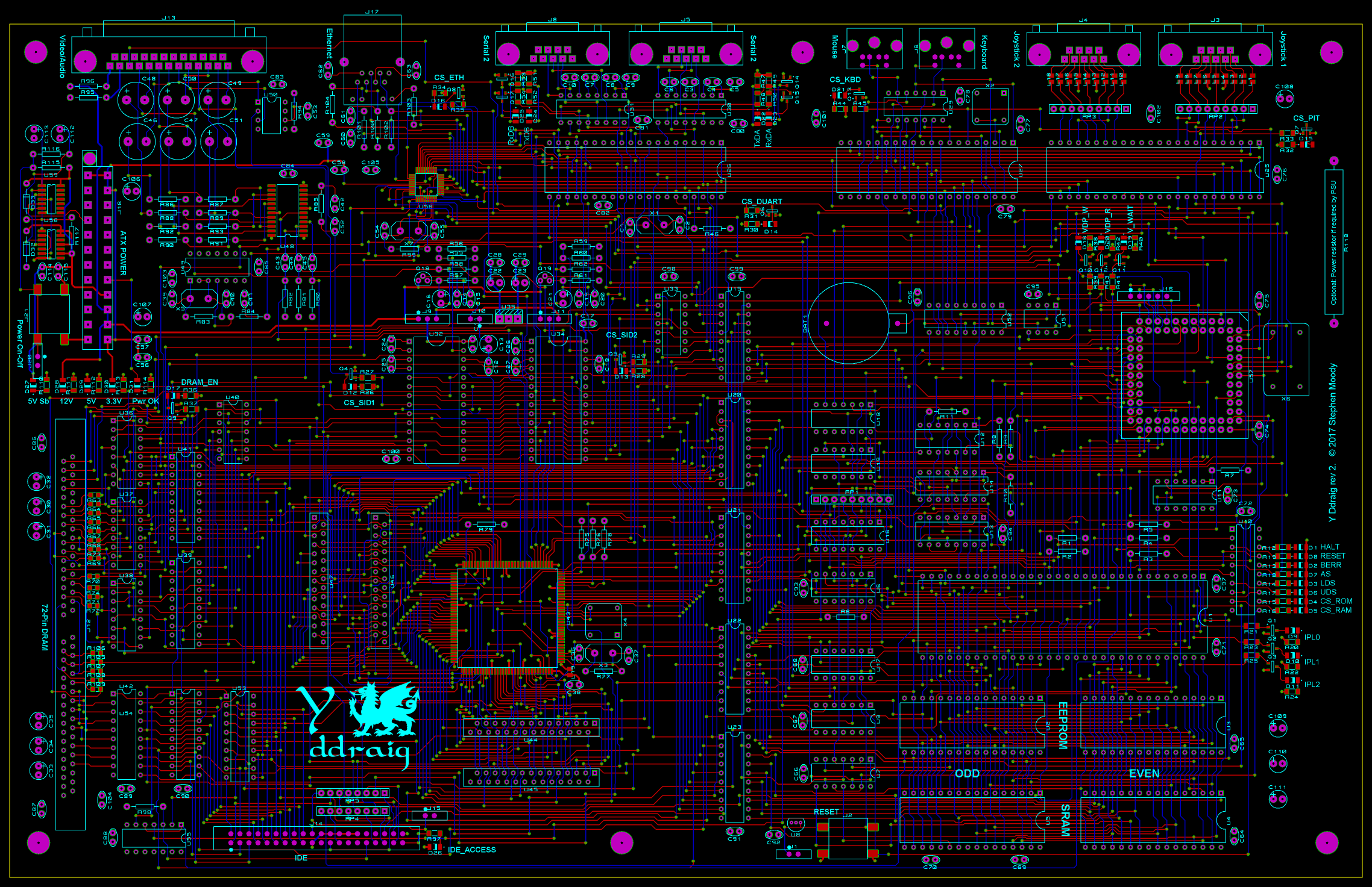
| Board Specs | |
|---|---|
| Layers | 4 |
| Size | 380mm x 240mm |
| Vias | 1615 |
| Holes | 3438 |
| Traces | 4627 |
I’m getting the PCB manufactured with EasyEDA as the board cost was reasonable for a 4 layer board of this size.
Once the boards have been delivered will post an update.