Address decoding
Before writing any software for Y Ddraig the CPLD will need to be programmed. The CPLD being used here is a Xilinx XC95108 and it is responsible for the address decoding for the peripherals and will eventually be used for controlling the DRAM but that isn’t going to be used in the inital stages of getting the computer up and running.
Clock generator
The clock signal for the 68000 is generated by CPLD so the first step is to create a clock signal for the 68000. The 10Mhz output clock is derived from the 40Mhz clock input to the CPLD.
architecture Behavioral of Clock is
	signal clk_divider : std_logic_vector(1 downto 0) := (others => '0');
begin
	process(clk)
	begin
		if (rising_edge(clk)) then
			clk_divider <= clk_divider + 1;
		end if;
	end process;

	clk10 <= clk_divider(1);
end Behavioral;
Address decoding
The memory map that is going to be used for Y Ddraig is as follows:
| Device | Start Address | End Address |
|---|---|---|
| Static Ram | 0x000000 | 0x0FFFFF |
| Dynamic RAM | 0x100000 | 0x900000 |
| DUART | 0xF7F000 | 0xF7F0FF |
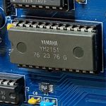
| YM2151 | 0xF7F100 | 0xF7F1FF |
| PIT | 0xF7F200 | 0xF7F2FF |
| KBD | 0xF7F300 | 0xF7F3FF |
| IDE | 0xF7F400 | 0xF7F4FF |
| ETHERNET | 0xF7F500 | 0xF7F5FF |
| RTC | 0xF7F600 | 0xF7F6FF |
| VDP | 0xF7F700 | 0xF7F7FF |
| ROM | 0xF80000 | 0xFFFFFF |
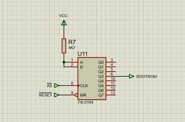
On startup the 68000 fetches two long word vectors from address 0x000000 for the stack pointer and start address for the code. As the ROM is set at address 0xF80000 this has to map the first four reads to the ROM.
This is handled by a 74LS164 8 bit shift register (U11) which sets the bootrom signal low for the first 4 address accesses (/AS) and then the bootrom signal is high until the next reset.
With this information the address decoding module is defined as follows:
entity AddressDecode is
    Port ( a          : in  STD_LOGIC_VECTOR (23 downto 8);
           clk        : in  STD_LOGIC;
           as         : in  STD_LOGIC;
           bootrom    : in  STD_LOGIC;
           reset      : in  STD_LOGIC;
           dtack      : out  STD_LOGIC;
           cs_rom     : out  STD_LOGIC;
           cs_sram    : out  STD_LOGIC;
           cs_duart   : out  STD_LOGIC;
           cs_pit     : out  STD_LOGIC;
           cs_kbd     : out  STD_LOGIC;
           cs_rtc     : out  STD_LOGIC;
           cs_ym2151  : out  STD_LOGIC;
           cs_eth     : out  STD_LOGIC;
           cs_vdp     : out  STD_LOGIC;
           cs_ide     : out  STD_LOGIC);
end AddressDecode;
ROM access is selected when the bootrom signal is 0 or the address range is in the ROM area. RAM access is similarly defined except that it expects the bootrom signal to be 1.
Peripheral access defined in 256 byte address blocks in the defined address ranges.
-- $F80000 - $FFFFFF
cs_rom    <= '0' WHEN as = '0'
    AND (bootrom = '0' OR std_match(a, "11111-----------"))
    ELSE '1';

-- $000000 - $0FFFFF
cs_sram   <= '0' WHEN as = '0'
    AND bootrom = '1' AND std_match(a, "0000------------")
    ELSE '1';

-- $F7F000 - $F7F0FF
cs_duart    <= '0' WHEN as = '0' AND std_match(a, "1111011111110000") ELSE '1';
-- $F7F100 - $F7F1FF
cs_ym2151   <= '0' WHEN as = '0' AND std_match(a, "1111011111110001") ELSE '1';
-- $F7F200 - $F7F2FF
cs_pit      <= '0' WHEN as = '0' AND std_match(a, "1111011111110010") ELSE '1';
-- $F7F300 - $F7F3FF
cs_kbd      <= '0' WHEN as = '0' AND std_match(a, "1111011111110011") ELSE '1';
-- $F7F400 - $F7F4FF
cs_ide      <= '0' WHEN as = '0' AND std_match(a, "1111011111110100") ELSE '1';
-- $F7F500 - $F7F5FF
cs_eth      <= '0' WHEN as = '0' AND std_match(a, "1111011111110101") ELSE '1';
-- $F7F600 - $F7F6FF
cs_rtc      <= '0' WHEN as = '0' AND std_match(a, "1111011111110110") ELSE '1';
-- $F7F700 - $F7F7FF
cs_vdp      <= '0' WHEN as = '0' AND std_match(a, "1111011111111111") ELSE '1';
For some of the peripherals the DTACK signal is automatically handled. These include the ROM (in hardware), the DUART and The PIT. For the others then the DTACK signal must be generated.
The DTACK generator:
signal dtack_s  : std_logic_vector(3 downto 0);

process (clk, reset, as)
begin
	if (reset = '0' or as = '1') then
		dtack_s <= (others => '0');
	elsif (rising_edge(clk)) then
		if (dtack_s < "1111") then
			dtack_s <= dtack_s + 1;
		end if;
	end if;
end process;
Check if we need to generate the DTACK signal:
-- Check the chip select signals to see if one is low
ack <= cs_sram AND cs_kbd AND cs_rtc AND cs_ym2151 AND cs_vdp AND cs_eth;

-- Generate the DTACK
dtack <= '0' WHEN ack = '0' AND dtack_s > "0101" ELSE '1';
This should provide the address decoding needed to be able be able to start writing some code to test the hardware is working as expected.